J-Link WiFi
JTAG/SWD debug probe with WLAN/WiFi interface
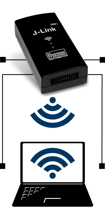
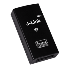
J-Link WiFi is a JTAG/SWD debug probe with WLAN/WiFi interface. It can communicate at high speed (up to 15MHz) with the supported target CPUs. If a wireless debug interface is required, J-Link WiFi is the perfect solution.

Overview
J-Link WiFi is the wireless option, when the targeted embedded device is moving or has to be shielded from the environment. It is USB powered, so that it can use the same power source as the target device. It can communicate at high speed with the supported target CPUs.
The J-Link debug probes are supported by all major IDEs including Eclipse, GDB-based IDEs and SEGGER Embedded Studio. For a complete list, please refer to Supported IDEs. J-Link is probably the most popular debug probe for ARM and RISC-V cores, making it the de-facto standard.
Key features
- Provides J-Link debugging for mobile applications
- Built-in VCOM functionality
- Comes with integrated licenses for: Unlimited breakpoints in flash memory (Unlimited Flash Breakpoints), RDI / RDDI and J-Flash
- Supports a broad range of microcontrollers
- Multiple CPUs supported—8051, PIC32, RX, ARM7/9/11, Cortex-A/R/M, RISC-V [More..]
- Supports direct download into RAM and flash memory
Why Use J-Link WiFi?
Mobility
Due to the WLAN/WiFi interface, the debug interface can also be used, if there is movement between the development PC and the target system. This is particularly useful in robotic applications.
Safety
In specific use cases, where the target system operates inside a hazardous environment, the wireless connection enables the developer to stay outside the dangerous area with his development system, even if there is a physical barrier between development and target system.
J-Link WiFi Licensing
J-Link WiFi comes with licenses for all J-Link related SEGGER software products: J-Link Unlimited Flash Breakpoints, J-Link RDI / RDDI, J-Flash, J-Link GDB Server, providing the optimum debugging solution for professional developers.
J-Link WiFi can be used with almost all ARM debuggers, enabling download to flash memory with an unlimited number of breakpoints when debugging programs located in flash memory of most popular ARM microcontrollers. It also comes with the license to use J-Flash, SEGGER's popular flash programming software.
Specifications
| Specification | Value | ||||
|---|---|---|---|---|---|
| Supported OS | Microsoft Windows (x86 / x64 / Arm64), Linux (x86 / x64 / Arm / Arm64), macOS (x64 / Apple Silicon) | ||||
| Electromagnetic compatibility (EMC) | EN 301 489-1/-17, EN 300 328, EN 62368 | ||||
| Operating temperature | +5°C ... +60°C | ||||
| Storage temperature | -20°C ... +65 °C | ||||
| Relative humidity (non-condensing) | Max. 90% rH | ||||
| Mechanical | |||||
| Size (without cables) | 103mm x 53mm x 28mm | ||||
| Weight (without cables) | 70g | ||||
| Available Interfaces | |||||
| WiFi interface | IEEE 802.11 b/g/n (2.4 GHz) | ||||
| USB interface | USB 2.0 (Hi-Speed) | ||||
| Target interface | JTAG / SWD 20-pin | ||||
| JTAG/SWD Interface, Electrical | |||||
| Power supply | USB powered, max. 220mA@5V | ||||
| Target interface voltage (VIF) | 1.2V ... 5V | ||||
| Current drawn from target voltage sense pin (VTRef) | < 25µA | ||||
| Target supply voltage | 5V (derived from USB voltage) | ||||
| Target supply current | Max. 300mA | ||||
| Reset type | Open drain. Can be pulled low or tristated | ||||
| Reset low level output voltage (VOL) | VOL <= 10% of VIF | ||||
| For the whole target voltage range (1.2V <= VIF <= 5V) | |||||
| LOW level input voltage (VIL) | VIL <= 40% of VIF | ||||
| HIGH level input voltage (VIH) | VIH >= 60% of VIF | ||||
| For 1.2V >= VIF <= 3.6V | |||||
| LOW level output voltage (VOL) with a load of 10 kOhm | VOL <= 20% of VIF | ||||
| HIGH level output voltage (VOH) with a load of 10 kOhm | VOH >= 80% of VIF | ||||
| For 3.6 <= VIF <= 5V | |||||
| LOW level output voltage (VOL) with a load of 10 kOhm | VOL <= 20% of VIF | ||||
| HIGH level output voltage (VOH) with a load of 10 kOhm | VOH >= 80% of VIF | ||||
| JTAG/SWD Interface, Timing | |||||
| Target interface speed | Max. 15 MHz | ||||
| SWO sampling frequency | Max. 30 MHz | ||||
| Data input rise time (Trdi) | Tfdi <= 20ns | ||||
| Data output rise time (Trdo) | Trdo <= 10ns | ||||
| Data output fall time (Tfdo) | Tfdo <= 10ns | ||||
| Clock rise time (Trc) | Trc <= 3ns | ||||
| Clock fall time (Tfc) | Trc <= 3ns | ||||


