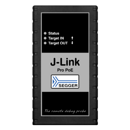
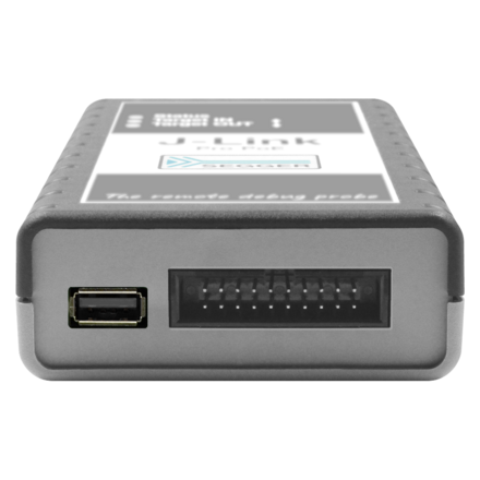
J-Link PRO PoE
The specialized high-end debug probe for test farms
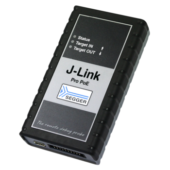
J-Link PRO PoE is SEGGER's specialized programming and debug probe for creating test farms. It can draw power via Ethernet and supplies power to the target either via debug interface or a USB A connector.
Overview
Quality assurance requires testing and when it comes to testing – more is better.
The power supply of test devices can be controlled remotely. This enables automated reboot for the testing process as well as the ability to turn off devices not in use, making it easy to build large-scale test farms.
The built-in web server makes manual configuration easy. Ethernet allows the use of the debug probe far away from the PC, over a hardwired or wireless network, in a development or production environment. It also makes download and debugging speeds higher and provides electrical isolation from the PC.
Key features
- PoE-enabled Ethernet interface
- Switchable power out via USB-A or 20-pin header
- Download speed up to 4 MB/s
- Unlimited breakpoints in flash memory (Flash Breakpoints)
- Use with Ozone, RDI/RDDI and J-Flash
- Comes with web interface for easy TCP/IP configuration (built-in webserver)
- Built-in VCOM functionality
- Supports a broad range of microcontrollers
- Supports direct download into RAM and flash memory
- Free software updates
What is a test farm?
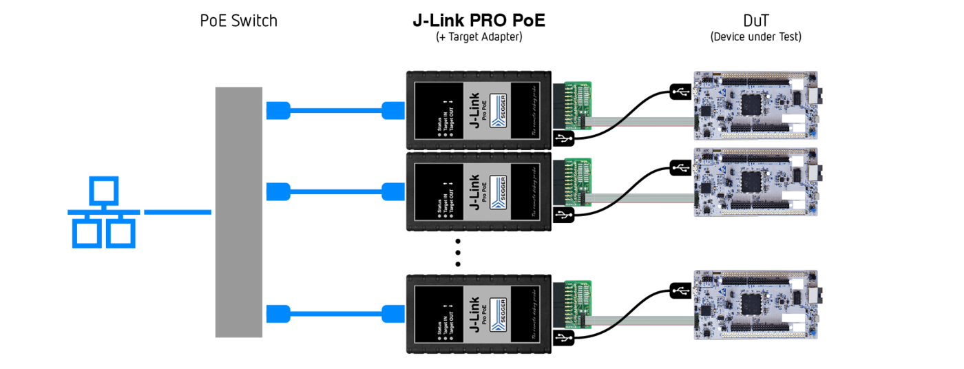
In terms of embedded systems, a test farm (or “board farm” or “device farm”) consists of a number of nodes (such as evaluation boards, prototype boards, production boards, finished products, etc.) connected to a network via debug probes, making them remotely accessible to testers or developers.
It is a very efficient way to share access to hardware that is in limited supply among a number of users. Additionally, automated build systems can run tests on the same standard setup, which is ideal for regression testing, continuous integration, compiler tests, and more.
Use cases
There are a lot of use cases for almost any test setup for an embedded system. As soon as the number of devices to be tested grows, a test farm is inevitably required to ensure quality. A test farm using J-Link PRO PoEs may consist of multiple test devices of the same type or be completely different. We have described a couple of test cases below.
Communication tests
Communication reliability can only be tested with massive test setups that generates a huge amount of traffic on the communication channel. Specifically, wireless traffic, using protocols such as WiFi, ZigBee or Matter, is prone to interference and requires thorough testing in order to ensure operation even under bad conditions. Communication test setups therefore use heterogeneous targets to ensure interoperability with different devices as well as a huge number of similar devices to prove reliability.
Compatibility tests
Testing compatibility of an updated firmware module running on different platforms or of a compiler requires a setup using different devices. A test farm shortens test time by addressing the tests in parallel on multiple different targets and ensures, that any changes to the compiler or firmware module are tested thoroughly against all possible target devices.
Supported devices
The J-Link PRO PoE as a member of the SEGGER J-Link debug probes supports a wide range of CPU cores. The list of supported manufacturers, families, and devices and SoCs includes tens of thousands of devices in hundreds of device families.
Device not listed? Please don’t hesitate to contact us.

Ethernet
J-Link PRO PoE features a PoE-enabled Ethernet interface as an alternative to the USB connection specifically to reduce the size of a cable harness in test farms.

Power & safety (galvanic isolation)
With PoE the J-Link PRO PoE can be powered and communicated with via a single interface. Target systems are shielded from power surges as the Ethernet signal lines provide galvanic isolation of the J-Link PRO PoE (and the target system) from the network and development PC.

Software
All software is included free of charge. It comes with licenses for all J-Link related SEGGER software products, such as J-Link Unlimited Flash Breakpoints, Ozone, RDI/RDDI, J-Flash, J-Link GDB Server, providing the optimum debugging solution for professional developers.
The J-Link Software and Documentation Package is available here:
Multi-platform
As a multi-platform solution, J-Link PRO PoE comes with the setup and control software for Linux, macOS and Windows. Software and firmware updates are included. Similarly, use on all currently supported target devices, and any that will be added, is also included.
J-Flash
J-Flash is a part of the J-Link Software and Documentation Package and allows the programming of the internal and external flash memory of a microcontroller-based embedded system via J-Link.

Flash Breakpoints
The J-Link PRO comes with an additional feature, called Unlimited Flash Breakpoints. Unlimited Flash Breakpoints allow the user to set an unlimited number of breakpoints when debugging in flash memory.

Ozone — The J-Link debugger
Standalone debugger
Ozone focuses on debugging. There are no compiler or project window distractions. All debug windows can be moved, resized and docked, to provide you with the workspace you need.
Ozone offers all well-known debug controls and information windows, and more. Instruction trace, power graph, live watches, and real-time terminal I/O further extend these capabilities.
Performance analyzer
With J-Link's High-Speed Sampling technology, Ozone can sample and visualize an embedded system's variables over time. Checking values and flags in the debugger, while the target keeps running, is easy.
J-Link's power measurement features enable you to record the power consumption of your target device in a debug session. This is especially helpful when you are developing a low-power device and need to know how power consumption changes when you enable or disable certain components.
Media gallery
Videos
Technical specifications
| General | ||||||||
|---|---|---|---|---|---|---|---|---|
| Supported OS | Microsoft Windows (x86/x64), Linux (x86/x64/Arm), macOS (x86/Apple M1) | |||||||
| Electromagnetic compatibility (EMC) | EN 55032, EN 55035 | |||||||
| Operating temperature | +5°C ... +60°C | |||||||
| Storage temperature | -20°C ... +65 °C | |||||||
| Relative humidity (non-condensing) | Max. 90% rH | |||||||
| Mechanical | ||||||||
| Size (without cables) | 123mm x 68mm x 30mm | |||||||
| Weight (without cables) | 125g | |||||||
| Available interfaces | ||||||||
| Ethernet interface | 100 Mbit/s | |||||||
| PoE supply voltages | IEEE 802.3af PoE type 1, class 3 | |||||||
| USB interface | USB 2.0 (Hi-Speed) | |||||||
| Target interface | JTAG/SWD 20-pin USB-A (power only) | |||||||
| JTAG/SWD interface, electrical | ||||||||
| Target interface voltage (VIF) | 1.2V ... 5V | |||||||
| Current drawn from target voltage sense pin (VTRef) | < 25µA | |||||||
| Target supply voltage | 5V (when powered via USB) 5.25V (when powered via PoE) | |||||||
| Target supply current | Max. 400mA (when powered via USB) 1000mA (when powered via PoE) | |||||||
| Reset type | Open drain. Can be pulled low or tristated | |||||||
| Reset low level output voltage | VOL <= 10% of VIF | |||||||
| For the whole target voltage range (1.2V <= VIF <= 5V) | ||||||||
| LOW level input voltage (VIL) | VIL <= 40% of VIF | |||||||
| HIGH level input voltage (VIH) | VIH >= 60% of VIF | |||||||
| For 1.2V >= VIF <= 3.6V | ||||||||
| LOW level output voltage (VOL) with a load of 10 kOhm | VOL <= 20% of VIF | |||||||
| HIGH level output voltage (VOH) with a load of 10 kOhm | VOH >= 80% of VIF | |||||||
| For 3.6 <= VIF <= 5V | ||||||||
| LOW level output voltage (VOL) with a load of 10 kOhm | VOL <= 20% of VIF | |||||||
| HIGH level output voltage (VOH) with a load of 10 kOhm | VOH >= 80% of VIF | |||||||
| JTAG/SWD interface, timing | ||||||||
| Target interface speed | Max. 50 MHz | |||||||
| SWO sampling frequency | Max. 100 MHz | |||||||
| Data input rise time (Trdi) | Trdi <= 20ns | |||||||
| Data input fall time (Tfdi) | Tfdi <= 20ns | |||||||
| Data output rise time (Trdo) | Trdo <= 10ns | |||||||
| Data output fall time (Tfdo) | Tfdo <= 10ns | |||||||
| Clock rise time (Trc) | Trc <= 3ns | |||||||
| Clock fall time (Tfc) | Trc <= 3ns | |||||||
| Analog power measurement interface | ||||||||
| Sampling frequency | 200 kHz | |||||||
| Resolution | 50 uA | |||||||
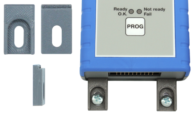
Mounting brackets
SEGGER's mounting brackets provide a reliable solution for securely fastening Flasher in-circuit programmers during use. Designed for stability and ease of use, these brackets also ensure a tidy and professional setup for test farms using J-Link PRO PoE debug probes.
The mounting brackets are available directly from the SEGGER shop.
Alternatively, we offer the option to 3D print the mounting brackets yourself. A downloadable ZIP file is provided, containing a STEP file for modifications, an STL file ready for 3D printing, and a PDF with detailed dimensions.
FAQ
Q: Can I use J-Flash with J-Link PRO?
A: Yes. J-Link PRO comes with a license for J-Flash preinstalled on the probe itself. No license setup necessary, simply plug in J-Link PRO and start using J-Flash.
Q: What is the advantage of J-Link versus simple probes such as FTDI-based systems?
A: J-Link has numerous advantages: the actual J-Link software supplied by SEGGER (which enables use with common IDEs), the availability of Unlimited Flash Breakpoints for the debugging of software which runs in the flash of microcontrollers, it’s high speed and it’s simple, fast download into flash memory.
In contrast to most simple probes, J-Link supports adaptive clocking as well as SWD and SWO. It also functions more stably, since it is not just a dump USB to JTAG converter. Instead, it uses the intelligence of the built-in CPU which provides more robust communication. This is especially so in situations where the target CPU runs at low clock speeds.
Q: May I work with more than one J-Link at the same time, on the same machine?
A: Yes, you can connect an unlimited number of J-Links to your PC. No special configuration required; each J-Link is registered with its unique serial number on the PC. This enables you to have multiple J-Links connected at once.
Q: I have multiple Arm cores in my JTAG chain. How can I debug them (simultaneously) with J-Link?
A: That's simple: Two or more debuggers can use the same J-Link simultaneously. Multi-core debugging requires multiple debuggers or multiple instances of the same debugger. You need to tell your debugger which device in the scan chain you want to debug. Additional special settings are not required.
Q: Does J-Link support the Embedded Trace Buffer (ETB)?
A: Yes. J-Link supports ETB on Cortex-M3/M4/M7 and Cortex-A/R (if implemented by target device).
Q: Does J-Link support the Micro Trace Buffer (MTB)?
A: Yes.
Q: Does J-Link support the Embedded Trace Macrocell (ETM)?
A: No. ETM requires another connection to the ARM chip and a CPU with built-in ETM. ETM is supported by the J-Trace product family.
Q: What is the maximum voltage that can be handled by the galvanic isolation of the Ethernet?
A: The Ethernet data lines are isolated as required per IEEE 802.3 (test voltage 1500 Vrms for one minute). Note that this is NOT valid for the Ethernet shield that has a direct electrical contact to the USB shield and a resistive and capacitive coupling to probe GND. For an effective isolation, you need to use an unshielded twisted pair Ethernet cable.


