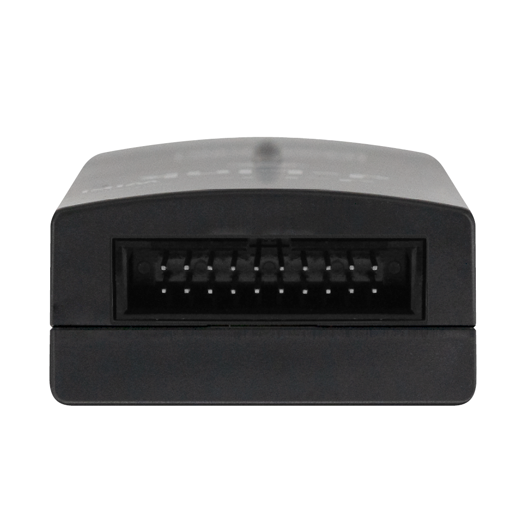
J-Link BASE
The JTAG/SWD debug probe with USB interface
The BASE version of the market-leading debug probe family. Top models of the J-Link family are J-Link PRO PoE, J-Link PRO, J-Link ULTRA+, and J-Link PLUS.
J-Link BASE is available in two form factors with identical function: J-Link BASE Classic and J-Link BASE Compact.

Overview
J-Link BASE is a USB-powered JTAG debug probe supporting a large number of CPU cores. Based on a 32-bit RISC CPU, it can communicate at high speed with the supported target CPUs. J-Link is used around the world in tens of thousand places for development and production (flash programming) purposes.
The J-Link debug probes are supported by all major IDEs including Eclipse, GDB-based IDEs and SEGGER Embedded Studio. For a complete list, please refer to supported IDEs. Including all models, more than 1,000,000 J-Links have been shipped so far, making J-Link probably the most popular debug probe for Arm cores and the de-facto standard.
Key features
- Download speed up to 1 MB/s
- Built-in VCOM functionality
- Supports a broad range of microcontrollers
- Free software updates
Supported devices
The J-Link BASE as a member of the SEGGER J-Link debug probes supports a wide range of CPU cores. The list of supported manufacturers, families, and devices and SoCs includes tens of thousands of devices in hundreds of device families.
Device not listed? Please don’t hesitate to contact us.
Software
All software is included free of charge. The J-Link Software and Documentation Package is available here:
License upgrade
The J-Link BASE offers basic functionality. To use the full range of functions of a J-Link PLUS, for instance, the J-Link Upgrade BASE to PLUS is needed.
This license upgrade comes with a software bundle that includes the J-Flash / J-Flash SPI license, software to program EEPROM and flash chips in Arm systems, as well as a J-Link Unlimited Flash Breakpoints license. Included is also the Ozone J-Link Debugger & Performance Analyzer, the Monitor Mode Debugging technology, the J-Link RDI / RDDI license, and the license pack for the RDI / RDDI interface.
The J-Link upgrade BASE to PLUS is available at shop.segger.com.
Multi-platform
As a multi-platform solution, J-Link BASE comes with the setup and control software for Linux, macOS and Windows. Software and firmware updates are included. Similarly, use on all currently supported target devices, and any that will be added, is also included.
Media gallery
Product photos


Videos

Mar. 2022 | 5:24 min
J-Link — J-Link Configurator

Aug. 2016 | 1:33 min
BBC micro:bit J-Link Upgrade — Intro

Jan. 2022 | 4:02 min
J-Link — Performance analysis

Mar. 2019 | 4:35 min
J-Link Remote Server — Intro

Mar. 2022 | 7:48 min
J-Link — J-Link Commander
Technical specifications
| General | |
|---|---|
| Supported OS | Microsoft Windows (x86/x64), Linux (x86/x64/Arm), macOS (x86/Apple Silicon) |
| Electromagnetic compatibility (EMC) | EN 55022, EN 55024 |
| Operating temperature | +5°C ... +60°C |
| Storage temperature | -20°C ... +65 °C |
| Relative humidity (non-condensing) | Max. 90% rH |
| Mechanical | |
| Size of J-Link BASE Classic (without cables) | 100mm x 53mm x 27mm |
| Weight of J-Link BASE Classic (without cables) | 70g |
| Size of J-Link BASE Compact (without cables) | 46mm x 46mm x 17mm |
| Weight of J-Link BASE Compact (without cables) | 20g |
| Available Interfaces | |
| USB interface (J-Link BASE Classic) | USB 2.0 (Hi-Speed); USB Type B |
| USB interface (J-Link BASE Compact) | USB 2.0 (Hi-Speed); USB-C |
| Target interface | JTAG/SWD 20-pin |
| JTAG/SWD Interface, Electrical | |
| Power supply | USB powered Max. 50mA + Target Supply current. |
| Target interface voltage (VIF) | 1.2V ... 5V |
| Current drawn from target voltage sense pin (VTRef) | < 25µA |
| Target supply voltage | 5V (derived from USB voltage) |
| Target supply current | Max. 300mA |
| Reset type | Open drain with 100 Ohms series resistor. Can be pulled low or tristated |
| Reset low level output voltage | VOL <= 10% of VIF |
| For the whole target voltage range (1.2V <= VIF <= 5V) | |
| LOW level input voltage (VIL) | VIL <= 40% of VIF |
| HIGH level input voltage (VIH) | VIH >= 60% of VIF |
| For 1.2V >= VIF <= 3.6V | |
| LOW level output voltage (VOL) with a load of 10 kOhm | VOL <= 10% of VIF |
| HIGH level output voltage (VOH) with a load of 10 kOhm | VOH >= 90% of VIF |
| For 3.6 <= VIF <= 5V | |
| LOW level output voltage (VOL) with a load of 10 kOhm | VOL <= 20% of VIF |
| HIGH level output voltage (VOH) with a load of 10 kOhm | VOH >= 80% of VIF |
| JTAG/SWD Interface, Timing | |
| Target interface speed | Max. 15 MHz |
| SWO sampling frequency | Max. 30 MHz |
| Data input rise time (Trdi) | Trdi <= 20ns |
| Data input fall time (Tfdi) | Tfdi <= 20ns |
| Data output rise time (Trdo) | Trdo <= 10ns |
| Data output fall time (Tfdo) | Tfdo <= 10ns |
| Clock rise time (Trc) | Trc <= 3ns |
| Clock fall time (Tfc) | Trc <= 3ns |
Assembly dimensions
The compact variant of the J-Link BASE is designed to mount securely and unobtrusively into development or end user equipment. The small size and two mounting holes enable placing the J-Link BASE Compact into existing equipment housings or to reserve space for direct-to-PCB mounting.
Typical applications are test fixtures that are used to automate firmware verification during development, or long-term test setups. It also can be used for integrated firmware reflash or service purposes inside end equipment, minimizing the number of tools that service technicians must carry around.


Package content
J-Link BASE Classic


J-Link BASE Compact


FAQ
Q: Can I use J-Flash with J-Link BASE?
A: No. You either need the additional license J-Link Upgrade BASE to PLUS in case you already own the product. Another option is to buy a higher-end model, such as J-Link PLUS, J-Link ULTRA+, or J-Link PRO.
The same applies to the J-Link Flash Breakpoints technology or the J-Link Debugger Ozone, for instance. Learn more here...
In order to receive a free 30 days trial license, please send an email including the J-Link serial number to: sales@segger.com.
Q: What is the advantage of J-Link versus simple probes such as FTDI-based systems?
A: J-Link has numerous advantages: Communication is handled by the probe which makes communication more reliable and faster. Flash loaders are provided by SEGGER or can be created using the device support kit. The debug communication interface RTT is available. All popular IDEs include support for the J-Link across all vendors. With an additional license an unlimited number of breakpoints in flash memory can be set. In contrast to most simple probes, J-Link supports adaptive clocking as well as SWD and SWO.
Q: May I work with more than one J-Link at the same time, on the same machine?
A: Yes, you can connect an unlimited number of J-Links to your PC. No special configuration required; each J-Link is registered with its unique serial number on the PC. This enables you to have multiple J-Links connected at once.
Q: I have multiple Arm cores in my JTAG chain. How can I debug them (simultaneously) with J-Link?
A: That's simple: Two or more debuggers can use the same J-Link simultaneously. Multi-core debugging requires multiple debuggers or multiple instances of the same debugger. You need to tell your debugger which device in the scan chain you want to debug. Additional special settings are not required.
Q: Does J-Link support the Embedded Trace Buffer (ETB)?
A: Yes. J-Link supports ETB on Cortex-M3/M4/M7 and Cortex-A/R (if implemented by target device).
Q: Does J-Link support the Micro Trace Buffer (MTB)?
A: Yes.
Q: Does J-Link support the Embedded Trace Macrocell (ETM)?
A: No. ETM requires another connection to the ARM chip and a CPU with built-in ETM. ETM is supported by the J-Trace product family.